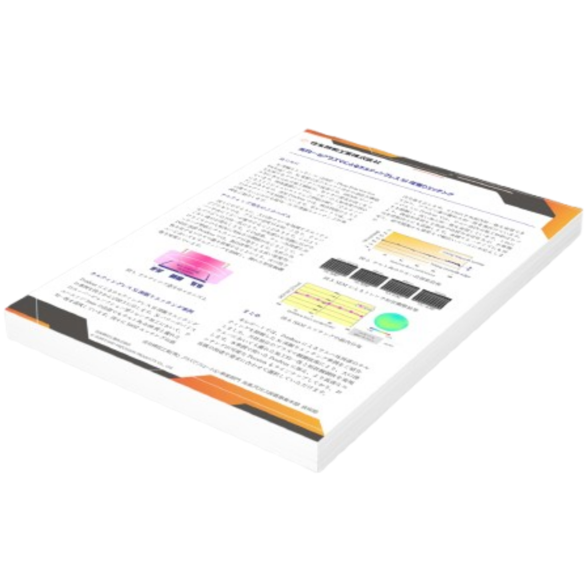

The precision required for deep silicon etching in devices such as MEMS continues to increase year by year. Among various challenges, "tilting"—a phenomenon where etched profiles become angled due to the oblique incidence of ions—is a key technical hurdle encountered when processing large-diameter wafers. Within-wafer profile non-uniformity directly impacts device yield and product consistency.
This report examines the underlying mechanisms of tilting from the perspectives of plasma density distribution and ion trajectories. Furthermore, it presents a case study demonstrating how Predeus—a silicon deep reactive-ion etching (DRIE) system equipped with a proprietary plasma source boasting exceptional density uniformity—effectively suppresses tilting even on large-diameter wafers.
Specifically, the report highlights superjunction trench etching for silicon power devices, providing evaluation results of tilt angles across various wafer positions alongside SEM cross-sectional observations of the trench profiles. Within-wafer uniformity data for SiO₂ etching is also included to validate the plasma source's inherent uniformity. Please download and refer to the full report for comprehensive numerical data and high-resolution SEM micrographs to support your process development from R&D through to high-volume manufacturing.